How is a picture taken?
You’re lining up your phone to take a picture of your dog. Light comes down from the sun, bounces off the dog, and into your camera lens, allowing you to take the photo. Your eyes work similarly, taking in all the light particles—known as photons—that are scattering off of objects in the world. Most things see by detecting these bouncing photons, which is why both you and your phone have a hard time seeing anything at all when the lights are off.

Electrons are the new photons
If two objects are brought close enough to each other under the right conditions, electrons from one object are transferred to the other. What’s useful is that these electrons don’t suffer the same problem the photons do. Even if two objects are incredibly close—such as two neighboring atoms—it is possible to detect which electron came from which atom.
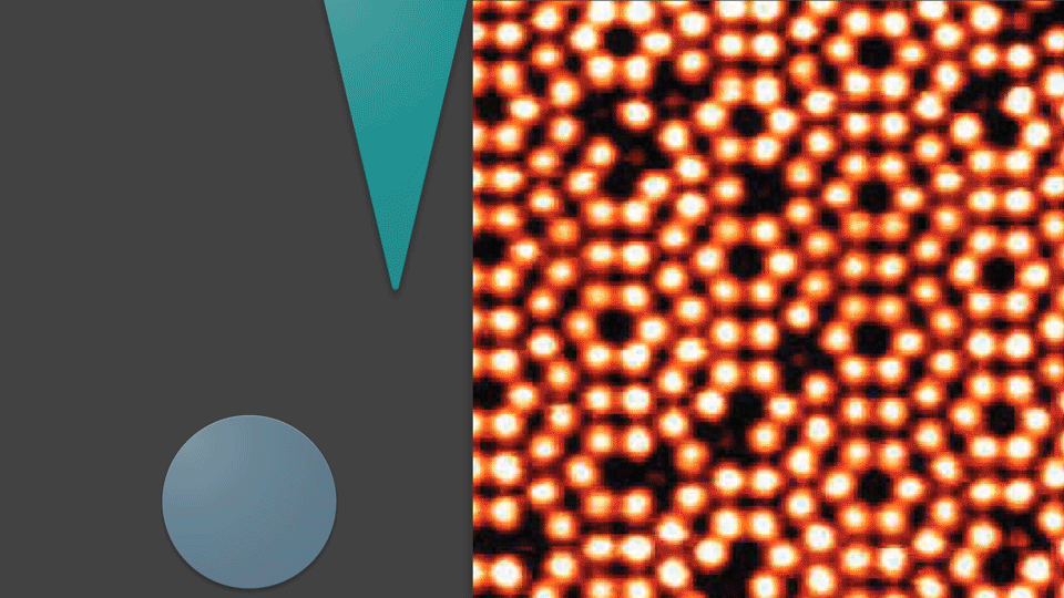
So instead of seeing with photons—like a normal camera—atoms are seen with electrons. Since the particle being used is different, the “camera“ will need to be different as well. Traditional cameras have a lens that lets the photons through. Electrons travel differently than photons—so instead of a lens, a sharp wire is used to pull electrons through to equipment that can detect them. If the wire is sharp enough at its tip, it will be able to tell which atom the electron comes from.

By moving this sharpened wire tip across a flat surface, electrons may be received from all of the objects present. This wire can image the shapes of atoms due to a special relation between how far an object is from the wire and how many electrons it will give up. Objects further away from the wire give only a few electrons, while objects really close to the wire will give it many electrons. The software connected to the wire will draw a picture based on the electrons it receives—coloring in bright spots where it counts a lot of electrons, and dark areas where it counts only a few electrons. This is how these atoms are detected, and how their picture is taken. With a camera, objects are seen by detecting the photons that bounced off of them. Atoms, however, are seen by detecting their electrons. So when the wire produces a photo, it is actually visualizing the electrons that the objects hold inside themselves. Using sharp wires to take pictures by detecting electrons from surfaces is a technique known as Scanning Tunneling Microscopy—or STM for short.
More than just a camera
The way that STM captures an image is pretty different from how a normal camera would. The unique way STM produces pictures not only enable it to image really small objects, but also allow it to do things normal cameras can’t. STM is not just for taking pictures.

If the STM tip is moved very close to an atom, interactions between the two will cause the atom to be attracted to the tip. The tip may then pick up the atom and drop it back off at another location. Using STM, scientists can manipulate individual atoms—controlling where they lie on a surface. Structures can be built, words can be spelled out, and even movies can be made by using atoms to draw characters.
STM is a powerful tool used to observe the smallest fundamental building blocks of our world. As technology trends towards smaller and smaller devices STM remains an important tool. Using it researchers can observe how materials are structured at an atomic level and build their own atomic sized devices.